
High Tech

Micron Opens Semiconductor R&D Facility in Boise

Published 9/15/2017

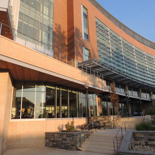
Micron Technology opened a $200 million semiconductor research and development facility in Boise in August of 2017. The four-story, 100,000-sf building will feature engineering laboratories with sophisticated manufacturing systems for the production of advanced memory chip technologies. Construction began on the project in October of 2015. Micron is also planning to build a three-story, 225,000-sf office facility on its Boise campus.  

Read More

Virtual and Augmented Reality are Reinventing Medical Education

Published 7/19/2017

Virtual and augmented reality are bringing new learning experiences to today’s medical students—and their campuses. The building boom is part of a revolution in the way medicine is taught. Today, medical students often learn with sophisticated mannequins, computer models, and collaborative electronic projects. Now, some schools are taking the technology a step further, building immersive environments where the doctors, nurses, and dentists of tomorrow can experience real medical settings and explore human anatomy in three dimensions.

Read More

Versum Materials Breaks Ground on R&D Laboratory

Published 6/3/2017

Versum Materials broke ground in May of 2017 on a research and development laboratory in Hometown, Pa. Part of a $20 million expansion of Versum’s chemical manufacturing campus, the project will support the synthesis and purification of molecules to enable the production of organometallic compounds used by the semiconductor industry. The lab will accommodate approximately 30 employees and is expected to open in late 2019.

Read More

Florida Advanced Manufacturing Research Center Opens in Kissimmee

Published 4/28/2017

The $75 million Florida Advanced Manufacturing Research Center opened in April of 2017 in Kissimmee. Created by the University of Central Florida in collaboration with Osceola County and the Florida High Tech Corridor Council, the 109,000-sf facility houses the world’s first industry-led smart sensor consortium.

Read More

Swansea University Constructs Computational Foundry

Published 3/6/2017

Swansea University began construction in February of 2017 on the £31 million Computational Foundry in Wales in the United Kingdom. Designed by AHR Architects to foster collaboration with industry and academic partners, the interdisciplinary facility will accommodate research and teaching programs in the computational and mathematical sciences. Housing over 150 investigators, the Computational Foundry will provide leading-edge experimental setups, sophisticated R&D labs, prototyping suites, conference rooms, lecture halls, and offices.

Read More

University of Sydney Opens Nanoscience Hub

Published 5/4/2016

The University of Sydney opened the AUD$150 million Sydney Nanoscience Hub in April of 2016. Housing the Australian Institute for Nanoscale Science and Technology (AINST), the facility features ISO Class 5 and Class 7 cleanrooms to support advanced research in photonics, engineered quantum systems, and energy technologies. Providing core labs as well as teaching space, the Nanoscience Hub accommodates device design, fabrication, and testing in a single location.

Read More

CoorsTek Constructs Research and Manufacturing Center

Published 4/7/2016

CoorsTek began building a $120 million research and manufacturing center in March of 2016 in Golden, Colo. The 300,000-sf facility will provide design labs, testing suites, and production space for the manufacture of ceramic components used in the automotive, defense, and semiconductor industries. The project is being built by Mortenson Construction and is expected to be fully operational by 2018.

Read More

Florida Advanced Manufacturing Research Center Builds Kissimmee Facility

Published 12/23/2015

Construction began in December of 2015 on the $71.4 million Florida Advanced Manufacturing Research Center in Kissimmee. Created by the University of Central Florida in collaboration with Osceola County and the Florida High Tech Corridor Council, the 109,000-sf facility will house the world’s first industry-led smart sensor consortium. Featuring a flexible cleanroom with adaptable walls and flooring, the project will provide a semiconductor foundry, a design center, and labs for the development of new technologies using integrated circuits.

Read More

AMS Plans Marcy Wafer Fab

Published 9/8/2015

AMS AG (formerly Austriamicrosystem) will begin construction in spring of 2016 on a 360,000-sf wafer fab in Marcy, N.Y. Located on the 428-acre Nano Utica site, the project will support the production of analog devices on 200mm to 300mm wafers. Constructed by Fort Schuyler Management, the development will include office buildings and support space for a total buildout of approximately 600,000 sf. Production is expected to begin in late 2017.

Read More

UMass Amherst Employs Core and Shell Strategy for Life Science Laboratories

Published 6/10/2015

Using a phased, core-and-shell strategy to construct the 310,000-gsf Life Science Laboratories (LSL) building allowed the University of Massachusetts Amherst to obtain high-level research space and take advantage of the competitive bid market and economic incentives available in 2010. The approach also provided economies of scale and the advantage of postponing programming and occupancy decisions with subsequent fit-outs.

Read More

Apple Plans Yokohama R&D Facility

Published 4/8/2015

Apple is planning to build a four-story, 269,000-sf research and development facility in Yokohama, Japan. Constructed on the site of a former Panasonic factory in Tsunashima-higashi, the sustainably designed project will feature highly efficient building systems, water recycling technologies, and a green roof. Construction is expected to commence by the end of 2015 with completion in 2016.

Read More

Stony Brook University Plans Innovation and Discovery Center

Published 4/2/2015

Stony Brook University is planning to build the $62 million Innovation and Discovery Center in the 246-acre Research and Development Park in Stony Brook, N.Y. Designed by Mitchell Giurgola Architects, the 200,000-gsf business incubator will provide laboratory and office space for innovative biotechnology and high-tech companies. Construction will begin in spring of 2016 and completion is expected within three years.

Read More

Apple Plans Global Data Center Headquarters

Published 2/18/2015

Apple is planning to invest $2 billion to develop a global data center headquarters in Mesa, Ariz. The project involves building out an existing 1.3 million-sf manufacturing facility and the completed structure will be powered entirely by sustainable energy sources.

Read More

Technology Plays Critical Role in Design of Medical Education Facilities

Published 4/30/2014

The kind of technology prevalent in today’s health sciences education requires a robust infrastructure that must be figured into a facility’s design during the budgeting and planning stages. Virtual simulation, virtual anatomy, tablet computers, 3-D stereographic display, software tools for collaboration, and touch interaction with LCD monitors—even the tried-and-true classroom technology, such as whiteboards, videoconferencing, telephone conferencing, dual-image large screen projection, large screen LCD monitors, and connectivity for personal devices—all require thoughtful consideration.

Read More

University of Connecticut Plans Innovation Partnership Building

Published 2/24/2014

The University of Connecticut began construction in June of 2015 on the 119,000-sf Innovation Partnership Building in Storrs. Designed by Skidmore, Owings & Merrill, the $170 million project will provide flexible laboratories to support collaborative R&D with industry partners in advanced manufacturing, materials science, cyber infrastructure, pharmaceuticals, and biotechnology.

Read More